

C) Nanomaterials
The advance of material sciences led to a plethora of novel semiconductors and nanostructures. Nearly every week new materials are synthesized and many of them are proposed for applications in electronics and optoelectronics, for instance for thin film photovoltaic cells or thin film electronics. One of the most important properties required for such applications is a sufficient conductivity, given by a long Drude scattering time τ and a small effective mass m*. The conductivity of thin films, however, is difficult to access by techniques that probe electrical currents across macroscopic distances (see Fig. 5).
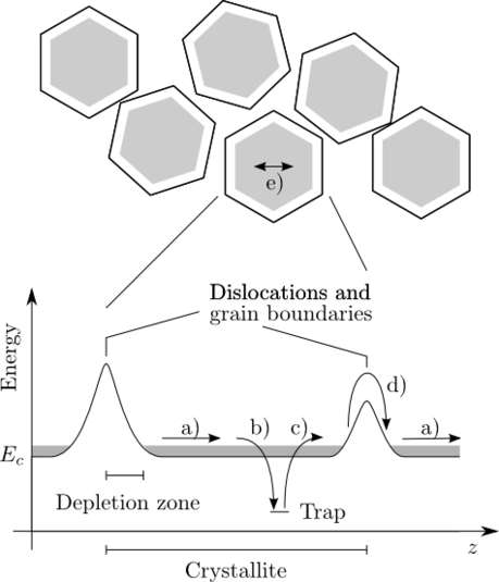 |
Fig 5: Illustration of transport processes in a polycrystalline thin film. Our research focuses on carrier drift caused by the material's inherent transport processes within the grains (a). In contrast to this, the macroscopic transport is slowed down by trapping and reemission of deep traps (b & c) and by the transfer across grain boundaries (d). The conceptual idea of THz measurements is that the radiation displaces the charge carrier on the scale of a few nanometers only (e), which makes scattering at grain boundaries improbable. Additionally, carriers bound in traps contribute only marginally to the polarization. |
Grain boundaries on the nanoscale and carrier trapping make classical characterization techniques such as Hall measurements impossible. Furthermore, the effective masses m* are unknown because the condition for cyclotron experiments ωct > 1 is not fulfilled. In contrast, THz radiation displaces charge carriers only on scales much smaller than the typical grain size. Scattering at grain boundaries is therefore suppressed and mobilities obtained from THz experiments can be orders of magnitude larger than those deduced by classical transport experiments across macroscopic distances. Additionally, THz radiation is insensitive to the slow dynamics of trapping and reemission. Altogether, time-resolved THz spectroscopy is an ideal tool for characterizing the material's inherent transport properties.
Figure 6 shows several examples of nanocrystalline semiconductors studied in our group. The main goal of the investigations is to deduce their Drude scattering times t and the carriers conductivity effective masses m*.
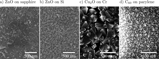 |
| Fig 6: SEM images of various nanocrystalline semiconductors fabricated in our group. |
In case of a pentacene thin film, we found a surprisingly low conductivity effective mass of the holes m* = 0.8 me. This explains the record mobility observed in our thin film (μ = 20 cm2/Vs), which exceeds the mobility obtained by electronic characterization by orders of magnitude. Altogether these results show that THz electromodulation spectroscopy yields the materials' inherent transport properties, where macroscopic techniques often fail because of grain boundary scattering and trapping.
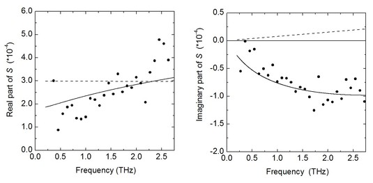 |
| Fig 7: Frequency dependence of the real and imaginary part of the THz modulation signal S. Experimental data are shown by symbols. The dashed lines are fits that follow the fundamental Drude model. A much better fit is obtained when the Bruggeman model is used. This yields a scattering time of 4.1 fs and a hole conductivity effective mass of 0.8 me. |